Wherever you are, you likely have devices containing a semiconductor chip around you – computers, phones, television sets, printers, cars, trains, airplanes, and more. It’s almost hard to believe that this tiny electronic component unleashed the same magnitude of change as the Industrial Revolution by making the computer revolution and the digital age a reality. And these semiconductor chips are everywhere; today, there are more chips in existence than people on earth.
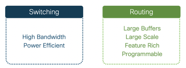
As a critical building block of networking devices, silicon chipset design primarily addressed routing use cases, and chipsets were optimized for programmability, deep buffering, and scale. When enterprises and cloud providers needed higher bandwidth, silicon designs emerged optimized explicitly for high-bandwidth and low power consumption. They met an immediate need, but at the expense of programmability, buffering, and scale.

Different silicon chipset requirements pushed the industry down a trajectory of two separate markets – the switching and routing markets – each of them defined by unique architectures, systems, and software. Despite several attempts to converge these into a single architecture, they have remained separate. Until today, switching silicon has always been faster than routing silicon.
While the industry searched for a convergence point, it grappled with the slowdown of “laws” that governed the development of silicon chipsets. For decades, the economics of silicon have been guided by 1) Moore’s Law – the number of transistors on a single silicon chip would double every two years and 2) Dennard Scaling’s Law – as transistor dimensions shrank, each transistor would operate faster and use less power. These two laws drove the golden age of silicon chipsets, but they are showing signs of weakness. As a result, silicon designs – for both routing and switching – have diverged as companies tried to overcome the limitations of Moore’s and Dennard’s Laws in their own way.
As innovators, and despite the mounting challenges, we never stopped dreaming of a single chipset architecture that could serve the needs of routing and switching. Could we build one architecture to solve multiple market needs, form factors, roles within the system, and that could scale, as needed? And could we do it all without making any compromises?
If we could build it, it would mean a fundamental shift in the industry.
Today, I’m thrilled to announce Cisco Silicon One™- a ground-breaking, new silicon architecture that has achieved these lofty goals.
For the first time, not only are we elevating routing silicon’s performance to the same level as switching silicon’s performance – both from a bandwidth and power efficiency perspective – but we are also paving the way to faster performance gains in the near future.
Cisco Silicon One is the first architecture that serves several different market segments – service provider and web-scale. And with future product lines built on a consistent silicon architecture, customers can enjoy ONE experience across the entire network, across all network functions and covering all form factors. With Cisco Silicon One, customers can significantly reduce OpEx – as network engineers save time on testing functionality, qualifying new hardware, and deploying new services with greater consistency and faster time-to-market.
Cisco Silicon One Q100, the first generation of this architecture, is twice the network capacity of all other high-scale routing ASICs. It is the first routing silicon to break through the 10Tbps benchmark for network bandwidth, without compromising carrier-class capabilities, e.g., feature richness, large queue set, deep buffers, large NPU tables, and advanced programmability.
It also demonstrates many architectural advantages. It can support a fixed switch or router with 10.8T worth of network ports up to large non-blocking distributed routers with Petabit scales. All of them with non-blocking performance, deep buffering with rich QoS, and programmable forwarding.
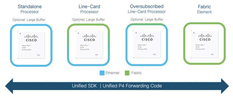
Another important innovation of the Cisco Silicon One Q100 is its unprecedented versatility. Up until now, networking vendors were using different and specific silicon chipsets for standalone processors, line card processors, and fabric elements.
But with the Cisco Silicon One Q100, all of these roles, including standalone network processor (optional deep buffers), traditional line card network processor (optional deep buffers), oversubscribed line card network processor (optional deep buffers), and fabric element in a distributed router can be met by a single chipset. All accomplished with a common and unified P4 programmable forwarding code and SDK.
And networks built with Cisco Silicon One Q100 will deliver greater consistency in features, services, and telemetry across multiple network locations because it unifies and streamlines operations by eliminating parity problems, upgrades, and other issues associated to different silicon.
The innovations in Cisco Silicon One represent years of investment and are vital for the future of the Internet. Legacy designs that rely simply on CMOS densities will suffer from the slowdowns inherent in Moore’s Law. With Cisco Silicon One, Cisco opens up a fast lane to future innovation that will outpace traditional methods while development cycles for silicon iterations will be dramatically shorter.
Embrace the future with Cisco Silicon One.


Very nice but where are the gory details described?
You want to make all component to unify, can only P4 to satisfy all scenario? and the other question is using HBM to make the deep buffer but the fabric needn’t this, so it will increase the cost of fabric?
Rochine,
Please see this note I posted to the P4 Slack channel.
https://p4-lang.slack.com/archives/C8Z5JAFJ5/p1576157664075400
Congratulations, Cisco.
P4 is poor with supporting stateful routing features. Prior Cisco routing silicon (CPP) used C to program the data plane. I suspect, Cisco ONE would still use C to program some routing features. The p4 compiler backend would be interesting work for this asic.
In the P4 Slack channel, a P4 expert has already asked if one can get an ODM switch using the Cisco 1 asic? When such details are available, please let us know at this blog or the P4 Slack channel – thanks.
I also maintain a list of all asics supporting a p4c (P4 compiler) backend and switches for the P4 community. The list is here:
https://github.com/hesingh/p4-info
The list only tracks hardware that supports P4-16.
Could Cisco let me know when Cisco 1 supports P4-16 and also a p4c backend? Then, I’d like to add the asic to the list – thanks.
Hi Rakesh: v. interesting. Can you please share silicon architecture details – Buffer Sizes, Latency, Programming Model (P4, Libs availability) etc.
Thanks
-Navneet
Can we test symmetric hash with P4-16 with the asic? Such a hash is used in Network Packet Broker (NPB).
We at BBL Foods, support and supply of hardly used batch type potato chips machines with an excellent working condition based on the capacity requirements.
Would add value, if you could please techno compare it with Nokia FP4 silicon capabilities, launched in June 2017..
Amazing, the future reach us!!
this will help