Solid State Drives (SSD) 101
In part one of this series we covered the internals of HDDs and some basic techniques manufacturers use to increase performance. In part two we are going into a deep dive of Solid State Drives (SSD), how they work, and some caveats.
Solid State Drives (SSD)
The solid-state drives (SSDs) have a simple unit where one or more bits are stored: the “NAND Flash Cell”. So, this should be easy! Right! Lets see.
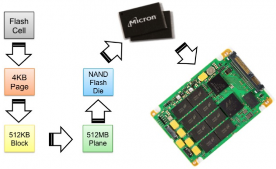
The SSDs are constructed like a Lego where the smaller piece is the “Flash Cell”. We aggregate multiple “Flash Cells” into a “4KB Page”. The amount of “Flash Cells” in a “Page” depends on the amount of bits the “Flash Cell” can manage. Now, here is the first caveat, a “Page” is the minimum writable unit in SSD. Even if you need to write a single bit, you would have to write an entire “4KB Page”.
We take “Pages” and group them into “512KB Blocks”. Here comes the second caveat, “Blocks” are the minimum erasable unit in SSD.
This causes a phenomenon known as the “write amplification” effect in SSD. If you need to erase a single bit, you need to modify and entire “Page” (the minimum writable unit), but you can only erase a “Block”. The drive needs to read the “128 Pages” that made the “Block”. Next it erases the “Block”, then write back the 127 unmodified “Pages” plus the 1 modified “Page”.
Finally, “Blocks” are aggregated into a “Plane”. Multiple “Plane” forms a flash die. Multiple die forms a chip and chips are used to create an SSD.
SSDs are not perfect, we already saw the “write amplification” but there are other caveats. You might have heard about SSD write wear. To understand it we need to understand the internals of a “NAND Flash Cell”.
A “NAND Flash Cell” is comprised of:
- A semiconductor material which can be manipulated to allow the flow of electrons through a channel
- A floating gate (where electrons are trapped to represent one or more bits)
- An oxide layer to isolate the floating gate and prevent electrons from escaping the floating gate
A control gate that when positively charged affect the semiconductor material allowing the flow of electrons through it

To “write” into a “NAND Flash Cell” the control gate is positively charge “opening” the channel at the P-Substrate (semiconductor material) allowing the flow of electrons from the source to the drain. Electrons are attracted by the positively charged control gate and through a mechanical phenomenon known as quantum tunneling {http://en.wikipedia.org/wiki/Quantum_tunneling}, some electrons will jump through the oxide layer and get trapped in the floating gate.
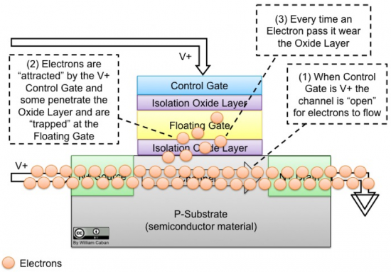
To erase the “NAND Flash Cell” a negative voltage is applied to the control gate and the electrons jump out of the floating gate. The “Flash Cell” will maintain its value (the electrons will remain at the floating gate) as long as no high voltage is applied to the control gate.
Every time electrons jump through the oxide layer the oxide is affected. Over time the wear of the oxide layer cause for some electrons to stay trapped at the floating gate and/or does not allow for enough electrons to jump into the floating gate. Eventually the system can not differentiate the “value” of the cell.
Because of this wear process there is a maximum amount of times a “Flash Cell” can be written. This is known as the write wear of the “Flash Cell”.
There are many “NAND Flash Cell” types with different write wear endurance. The number of times a “NAND Flash Cell” can be programmed and erased is known as the maximum number of program/erase cycles (P/E cycles).
| NAND Flash Cell Type | Bits | P/E Cycles | Vendors using it |
| Single Level Cell (SLC) |
1 |
~100,000 | Violin |
| Multi Level Cell (MLC) |
2 |
3,000 – 10,000 | Cisco UCS Invicta, FusionIO, Nimbus, PureStorage, Violin, NetApp |
| Triple Level Cell (TLC) |
3 |
1,500 – 2,500 | Consumer grade applications |
| Enterprise MLC (eMLC) |
2 |
20,000 – 30,000 | EMC XtremIO |
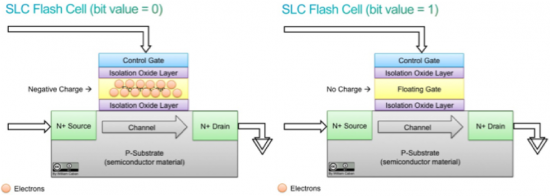
As seen in the previous table, a single-level cell (SLC) stores a single bit in the floating gate. If there are no charges in the floating gate, we say we have a bit value of one (1), if the floating gate has a negative charge, we say we have a bit value of zero (0).
For MLC with two bits, or TLC with three bits, the difference is that instead of determining if the floating gate has a negative charge or not, now, it has to read the voltage level of the floating gate to determine the stored value. But, for the same reason, it is more sensitive to “trapped” electrons and as such, lower P/E cycles.
The “Flash Cell” of a MLC and of an eMLC is basically the same. Some manufacturers use of thicker floating gate and thicker oxide layer for their eMLC to increase the P/E cycles. But, the main difference between the two is that eMLC is largely over-provisioned with many extra blocks (not visible to the host) to increase the overall drive endurance and eMLC includes embedded controllers to do wear leveling.
In the part 3 of this series we are going to cover additional storage concepts and general techniques used by the industry to increase performance of traditional storage systems.


Are you going into forced 4k alignment, dedupe, btl, GC, and async replication as well?
Yes, in post 4 I will go over some of these.